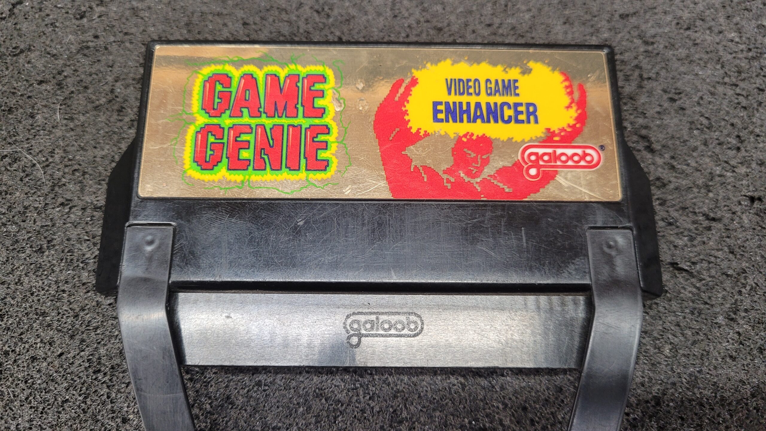
Inside the Galoob Game Genie (Model 7356) NES Under X-Ray
The Galoob Game Genie is one of the more elegantly deceptive pieces of consumer hardware from the early 1990s. From the outside it looks like a simple pass-through adapter and in a sense, that’s exactly what it is. But what happens electrically in between is what makes it interesting.
Designed by Camerica and distributed by Galoob, the NES Game Genie sits between the console and the cartridge via a pair of 72-pin connectors visible at the top and bottom edges of the X-ray. Electrically, it monitors the address bus and substitutes ROM data on the fly when it detects one of up to three intercepted addresses, all without touching the cartridge permanently.
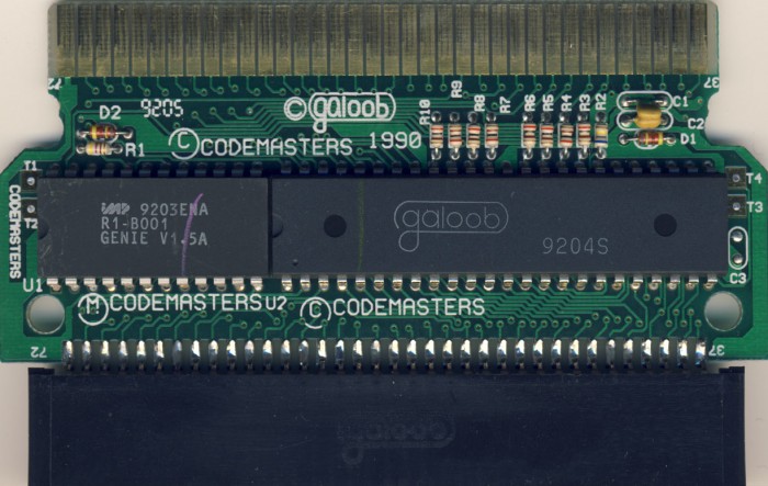
What the X-ray reveals is how sparse the design really is. The dominant feature is the large 48-pin custom ASIC the “Galoob” chip which handles all the real-time address comparison and data bus switching. To its right sits the smaller 24-pin ROM, which holds the 4 KB firmware that drives the code-entry menu. A handful of passives round out the board, including the 200-ohm resistors on the data lines that prevent bus conflicts when the ASIC asserts its own values.
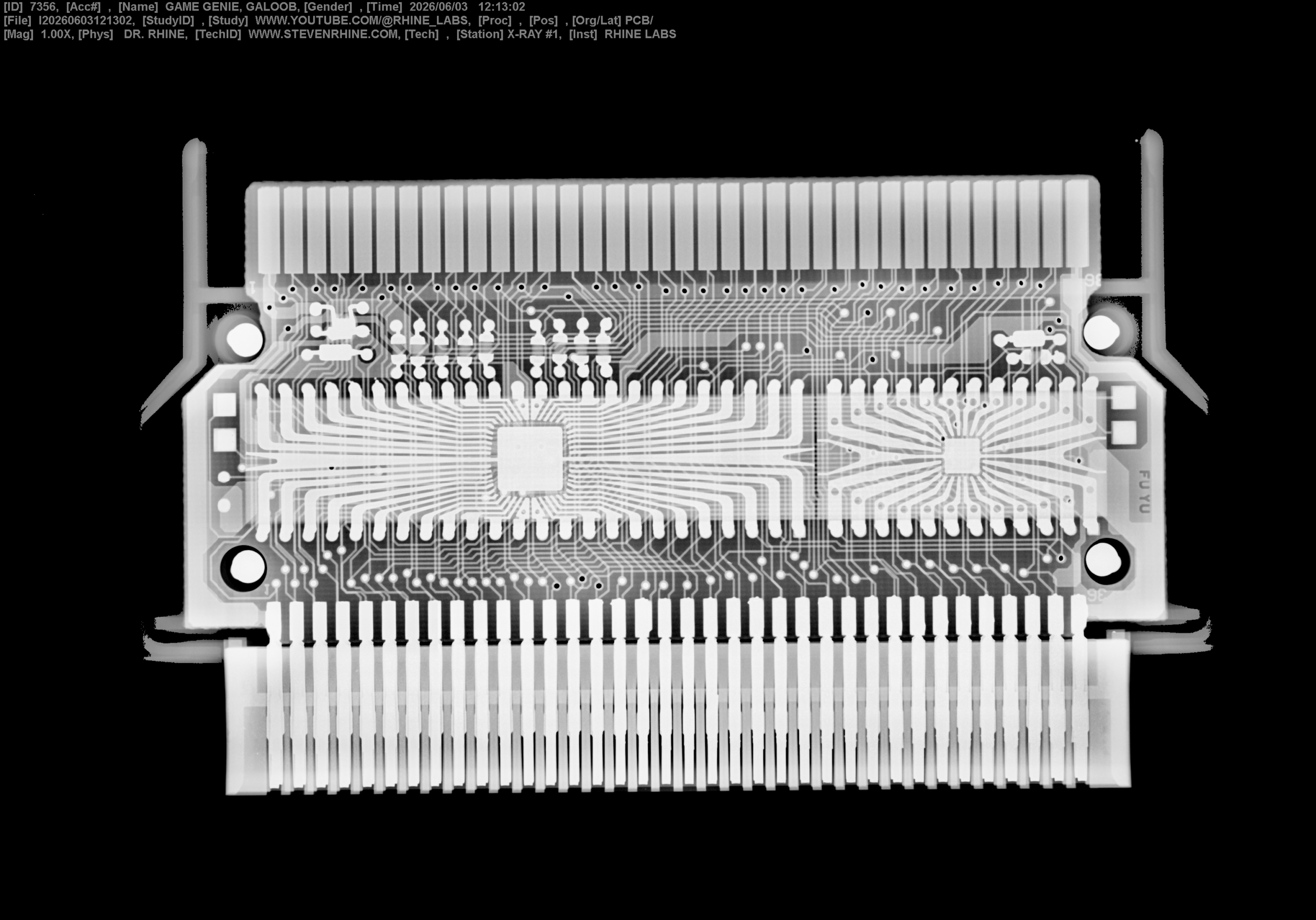
This is the discrete revision separate ASIC and ROM as distinct packages. Later units collapsed both into a single epoxy blob to cut costs. Under X-ray, those two chips and their routing tell the whole story: a minimal amount of custom silicon doing one very focused job at 1.79 MHz, invisibly, every single clock cycle the console is running.
Internal Photo Form NESCARTDB.com
For a device Nintendo tried to ban outright, the hardware is almost humble.
Last Updated on June 3, 2026 by Steven Rhine